

HDI printed circuit board affect manufacturing complexity
As the demands for electronic devices continue to increase, manufacturers need to shrink PCB sizes and maximize component density. One way to do this is by using HDI printed circuit boards. HDI technology is used in a variety of applications, from consumer electronics to aerospace and military equipment. The benefits of HDI technology include higher packing density, finer track structures and Microvias, and lower via and aspect ratios. However, implementing the necessary quality control protocols is essential for ensuring the performance and reliability of HDI circuit boards.
The manufacturing process of a multi-layer HDI PCB involves many intricate steps. The first step is layer build-up, which is accomplished by laminating sheets of insulating and conductive materials. The next step is microvia drilling, which uses laser drills to create small holes called “vias” for the connections between different layers of the board. The vias are then filled and capped, which reduces signal radiation and enables more precise metallization.
Another important step in the hdi printed circuit board manufacturing process is defining the structure of the board and selecting the right materials. The choice of materials has a significant impact on the overall performance of the PCB. Different laminates offer different dielectric properties, and designers must consider these factors during the design phase to ensure proper impedance control and signal integrity.
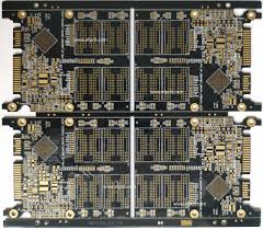
How does an HDI printed circuit board affect manufacturing complexity?
An HDI PCB requires more layers than a traditional PCB, and the number of layers depends on the complexity of the design. The design must also take into account the size of the components and the number of connections needed. It is important to use a good fanout strategy when designing an HDI PCB, as this will help minimize the number of sequential laminations required.
High-speed communication is a key application for HDI circuit boards. The smaller size and higher packing density of the board allow designers to place more components closer together, which increases signal transmission speed. The reduction in the size of the components themselves, coupled with the use of microvias and blind via technology, helps to further improve transmission speed.
In addition to the benefits of faster signal transmission, HDI PCBs are also more durable than traditional PCBs. They are more resistant to thermal expansion and physical shock, making them ideal for use in harsh environments. In fact, many automobiles today contain HDI circuit boards that monitor and control the motor, drive system, safety systems, and more.
Developing an HDI circuit board requires the use of multiple advanced fabrication processes and techniques, which can be expensive. This includes laser direct imaging, CAD/CAM software, special manufacturing equipment, and skilled operators. Detailed design rules that recognize impedance requirements, conductor widths, and hole sizes are also crucial for the success of an HDI design. In addition, thorough testing of the circuit board is vital to identify potential issues and ensure a high-quality end product. For these reasons, it is crucial to choose a reliable, experienced supplier when producing an HDI circuit board.