

PTH in circuit board assembly
A jiggling component or a loose screw can affect the functionality of a circuit board, so PCB assembly must be done carefully and accurately. Fortunately, automation can help reduce costs and human error at scale. Pick-and-place machines use mechanical or even vacuum-based movements to take a surface mount component from a feeder and put it in the correct position to be soldered, ensuring every joint is made correctly.
The machines can also handle a high volume of components and place them on multiple layers simultaneously, boosting efficiency. However, there are still certain types of components that require a more traditional method of assembly. One example is the through-hole (PTH) component, which requires a hole to pass its leads through for mounting and soldering. While PTH components are less common now than surface mount components, they’re necessary for some devices and applications.
The term “through-hole” refers to a type of hole in a printed circuit board that goes all the way through the entire circuit board, from one end to the other. These holes are used for connecting components and conducting electrical signals between different layers in the circuit board assembly. The holes are typically plated with copper, which gives them a lower-resistance path than would be possible without the copper plating. Plating the holes also eliminates dependence on contact alignment inside the hole, reducing resistance and making the connections more durable against vibration or temperature changes.
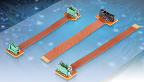
What is PTH in circuit board assembly?
Through-hole PCBs are particularly useful for high-power devices and for connecting different layers of the circuit board. They’re also more flexible than surface-mount devices, which are limited to a maximum number of layers. This is because the through-hole component’s leads are anchored by solder to the plated copper on the inside of the hole. This creates a stronger bond than just using glue or thermally conductive adhesives, and it ensures that the device’s power will always be directed where it’s needed.
During the PCB design process, it’s important to distinguish between plated through holes and non-plated through holes. The fabricator will only process a plated through hole if it is designed with a pad whose diameter is larger than the pin diameter of the corresponding through-hole component. To meet this requirement, the PCB design tool will add a solder stop mask to the pad. Circuit board assembly can be scaled easily to meet the demands of large-scale production. Whether for small batches or mass production, the process is adaptable and can be optimized for high-volume manufacturing.
Non-plated through holes, on the other hand, don’t have this pad feature and stand as simple holes in the circuit board. Mistaking a plated through hole for a non-plated through hole can cause the electrical charge to be misdirected, which can damage the circuit and potentially cause failures. To avoid this, make sure that the PCB designs you’re sending to the fabrication house clearly mark each as either a plated through hole or a non-plated through hole. This will keep the fabricator from mistakenly processing a through-hole for a non-plated through hole, which can be expensive and lead to manufacturing defects.