

Affect PCB Manufacturing Lead Times
A printed circuit board (PCB) is a vital component in all electronic devices and equipment. As design engineers are asked to create more new products in shorter periods of time, it becomes increasingly important to outsource PCB fabrication and assembly to a quality ECM partner with experience handling quick-turn projects. The right partners can provide fast turnaround and help minimize project delays caused by the complexities of the manufacturing process. To reduce pcb board manufacturing lead times, it’s helpful to understand the different factors that affect lead time, from initial fabrication and component procurement to the final assembly and testing stages.
Typical PCB manufacturing lead times are dictated by the availability of components and the complexity of the board’s layout. Component shortages have been plaguing the industry for some time, impacting common components like capacitors and resistors as well as specialized chips used in automotive systems. The fabricator should be aware of these issues and make sure that they have enough stocked components to produce the boards on time.
To optimize manufacturing lead times, the designer should work closely with their CM during the layout stage to make sure that the design meets the fabricator’s capabilities and production processes. This includes verifying that the fabricated board can handle the desired component density and ensuring that the layout allows for adequate room for a variety of potential mechanical constraints, such as hole size requirements for plated through holes and a sufficient margin between the silkscreen layer and traces to prevent ink bleeding into copper.
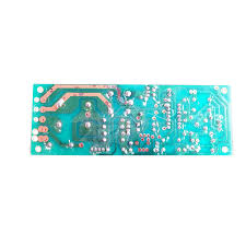
Factors That Affect PCB Manufacturing Lead Times
The fab drawing is an essential document for communicating the fabrication requirements of a PCB design to the fab house, including critical mechanical dimensions, IPC class, materials, layer stack-up, via drill chart, and plating thickness. Providing this documentation upfront to the fabrication house helps avoid costly rework during the manufacturing process and ensures that the design can meet manufacturing specifications.
Once the fab drawing is complete, it will undergo a design review and DRC check to determine whether it meets the tolerances and design rules of the PCB fabrication process. This ensures that the resulting boards will have proper connectivity and functionality. It also identifies any potential issues that could cause delays, such as traces that touch each other or have too skinny width, or holes that don’t match the intended locations on the PCB.
In addition to a clear fab drawing, the designer should supply their CM with the required PCB files in the correct formats. Doing this will ensure that all information is accurate and correctly translated between the two parties and can prevent lost or corrupted data that may occur when transferring files from one format to another.
The quickest way to reduce PCB production lead times is to keep the design as simple as possible and ensure that all relevant files are provided to the PCB manufacturer in advance of the start of the project. Keeping to the fabricator’s DFM guidelines also helps ensure that the resulting PCBs will meet the engineer’s specifications and can be assembled and tested as quickly as possible.