

key steps in PCB prototype design
The process of designing a PCB prototype involves several key steps, each crucial for ensuring that the final product will meet the intended requirements and function properly. A PCB prototype is a preliminary version of a printed circuit board created to test and verify the design before moving to full-scale production. The design of a PCB prototype requires careful planning, attention to detail, and a thorough understanding of both the electrical and mechanical aspects of the circuit. The key steps in PCB prototype design are essential to achieving a reliable and functional prototype.
The first step in PCB prototype design is conceptualizing the circuit and determining its specifications. This involves understanding the overall functionality of the product and selecting the necessary components, such as resistors, capacitors, microcontrollers, and connectors. The components should be chosen based on factors like power requirements, size limitations, and the specific application of the circuit. During this phase, it’s also important to consider the physical layout of the PCB and how the components will be arranged to ensure optimal performance and ease of assembly.
Once the components have been selected, the next step is to create a schematic diagram. A schematic is a graphical representation of the circuit that shows how the components are connected to one another. This is a critical stage in pcb prototype design because it defines the electrical connections and ensures that the circuit will function as intended. The schematic should be reviewed carefully to check for potential errors, such as incorrect connections or missing components. At this stage, it’s common to use computer-aided design (CAD) software to draw the schematic and make any necessary adjustments.
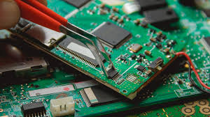
What are the key steps in PCB prototype design?
After finalizing the schematic, the next step is to convert it into a PCB layout. The PCB layout defines the physical arrangement of the components on the board and how the electrical traces will connect them. This is where the design begins to take shape as a tangible, real-world prototype. The layout process involves placing the components in a way that minimizes space while maintaining proper signal integrity and reducing the risk of interference. Proper routing of the electrical traces is essential to avoid issues such as crosstalk or signal degradation. The layout also needs to account for factors like power distribution and ground planes, which can affect the overall performance of the PCB prototype.
Once the layout has been designed, the next step is to perform a design rule check (DRC) to ensure that the board meets all manufacturing and electrical standards. DRC is a verification process that checks for potential errors such as trace width violations, clearance issues, or incorrect component placements. This step helps to avoid problems that could arise during the manufacturing process and ensures that the PCB prototype will be functional when assembled.
After the design has passed the DRC, the files are sent to a PCB manufacturer for fabrication. During this stage, the PCB prototype is physically produced, with the design transferred onto the PCB material. The fabrication process typically involves several steps, including etching the copper traces, drilling holes for through-hole components, and applying a solder mask and silkscreen. Once the prototype is fabricated, it undergoes assembly, where components are placed and soldered onto the board.
The final step in PCB prototype design is testing and validation. Once the PCB prototype has been assembled, it needs to be tested to ensure that it functions as intended. This involves checking the electrical connections, verifying the signal integrity, and conducting functional tests to ensure the prototype meets all specifications. If any issues are found, the design may need to be revised, and a new prototype may be created. Iterative testing and redesigning are often necessary to achieve the desired performance and reliability in the final product.
In conclusion, designing a PCB prototype involves several key steps, including conceptualizing the circuit, creating a schematic, developing the PCB layout, performing design rule checks, fabricating the PCB, and testing the final prototype. Each step plays an important role in ensuring that the prototype functions properly and meets the intended design requirements. Through careful planning and iterative testing, designers can create a reliable and effective PCB prototype that serves as the foundation for mass production.


